555 Timer Introduction
Over the next few posts, I want to introduce you to my favorite Integrated Circuit of all times, the NE555 timer chip. It isn’t new; it has been around since 1972. Here we are 50 years later, and according to Wikipedia, in 2017, over a billion of these are still being manufactured every year.
It’s incredibly versatile, very inexpensive, and just plain fun to play with. Several different companies are manufacturing several different versions, including the original NE555 and a CMOS version. They also are available in different packages that contain 1, 2 or even 4 of these chips in the same package, in this article, I’m only going to talk about the original NE555.
So what exactly is a 555 chip and what can you do with it? Let’s talk about those two things separately. In this post we will talk about the chip itself, and some basic details. In the articles that follow, we will build the circuits on an experimenter breadboard. Then we will play with changing some of the components and observe the changes that makes.
The NE555 Integrated Circuit
The NE555 comes in an 8 pin DIP, shown below. That means it is packaged in a Dual I-line Package. It has 2 rows of 4 pins, 8 pins in total. The spacing on the adjacent pins is .1 inches which fits perfectly in the various experimenters “breadboards” which are used to quickly hook a circuit up to experiment with it. My next article will go into more detail about that.

It also comes in a TO5-8 package.

This is a simple block diagram of the external connections, along with a list of what the normal abbreviations are and what each pin normally does.

1) GND; this is the ground pin; it would normally be hooked to the minus terminal of the battery or power supply.
2) TRG; this is the trigger pin. You supply a ground voltage here to trigger the timer.
3) OUT; this is the output pin
4) RESET; this is exactly what it sounds like; when it goes negative, the timer is reset.
5) CRTL; this is the control pin, sometimes it is just tied to ground thru a small value capacitor to prevent electrical noise problems.
6) THR; this is the threshold pin, shown grounded here.
7) DIS; this is the discharge pin
8) Vcc; this is hooked to the positive terminal of the battery or power supply.
This shows where each pin is PHYSICALLY located on the Integrated Circuit, usually just called an IC. Both of these show the pins looking down from the top of the IC.


The power needed to run a NE555 can be anywhere from 4.5 volts DC to 16 volts DC, some say up to 18 volts. The positive voltage is connected to the pin marked Vcc, and the negative voltage goes to the pin marked ground or GND.
The original NE555 can source or sink 200ma. What in the heck does THAT mean? OK, so if you have an IC, any IC, not just this one, the designers tell you how much current a particular IC can safely handle before it is damaged by excessive heat. The ORIGINAL NE555 (NOT the CMOS version) can source 200 milliamps (ma), and can also sink 200ma.
SOURCING means that a load, like an LED for example, hooked from pin 3, the output pin, to ground, can handle, in theory, 200ma safely before the IC destroys itself. So when the IC was active, in other words, pin 3 had a digital high voltage on it, that would make the LED light, but the current should be limited to under 200ma.
SINKING would mean just the opposite. That would mean that the load would be hooked from the Vcc to the output at pin 3 and would only light up when the output pin was LOW. Once again you need to limit the current to less than 200 ma.
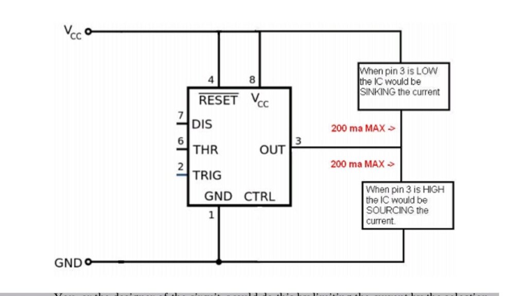
You, or the designer of the circuit, would do this by limiting the current by the selection of the load. For example, if the load was an LED, you would choose the correct size RESISTOR to put in series with the LED. If the load was say, a motor, you would need either a relay or a driver transistor at the output, so that the current coming out of the NE555 was below 200ma.
If you are interested in more information on the internal workings of the 555, Wikipedia has some good info. Just search on “Wikipedia 555 Timer”. Here, we are going to be looking more at what we can do with the 555.
Today we will be looking at brief descriptions of the different operation modes. For the next article we will hook up some circuitry and demonstrate how changing some components changes the frequency and the duty cycle.
Different Operating Modes
The 555 has several different modes of operation; monostable, bistable, and astable, are the most common. First we will talk about running the 555 in Astable Mode, also called Free Running Mode.
When used in the astable mode, the output voltage does not have a stable state. In other words, the output at pin 3 continually flips back and forth between a high state and a low state. This astable state will run continuously as long as power is supplied.
The diagram below shows how we configure the 555 to run in astable mode.

The ratio of high output to low output is called the “duty cycle”. The number of cycles, one complete high pulse and one complete low pulse, per second is called the “frequency”. Both the frequency and the duty cycle are set by the components R1, R2, and C. So for example, if we choose values that caused our 555’s output to go high, low, high, low, etc, 1000 times in one second, the frequency would be 1000 hertz. In old school terms, that was called 1000 cycles per second.
The drawing below shows two waveforms. The one at the top represents a 50% duty cycle because the width of the high pulses is the same as the low pulses.
The waveform on the bottom shows a duty cycle of 66.6% because the time of the high pulse is twice the size of the low pulse

Monostable Mode
In the monostable mode, the output has one stable state with the output voltage low. When it is triggered by a negative input on pin 2, the output goes high for a predetermined amount of time and then returns to the low state. The amount of time is determined by resistor R and capacitor C.

Bistable Mode
In the bistable mode, the output starts out low and stays there until it is set, causing the output to go high. It remains high until it receives a reset input, at which time it goes low again. So it has two stable states. In this example, the SET switch, at pin 2, makes the output go high and lights the green LED. The RESET switch, at pin 4 resets the output to a low state, turning on the red LED.

In the next article, we will look at the 3 circuits above, along with a few others, as we build them on a breadboard. Then we will change some values while observing the effects.